cuBLAS Worklog: Tối ưu GEMM theo kiến trúc phần cứng cho NVIDIA Tensor Cores
Note: Bài viết này là quá trình mình nghiên cứu nên có nhiều thuật ngữ liên quan đến CUDA, GEMM, kiến trúc GPU và deep learning, nên mình viết bằng tiếng Anh để giữ ý nghĩa kỹ thuật chính xác và dễ tra cứu hơn. Vì viblo content giới hạn 70000 từ nên bài viết này ko đầy đủ, mn có thể truy cập link đầy đủ ở cuối bài nếu muốn xem thêm.
Lời cảm ơn mọi người đã đọc bài viết của mình. Mình rất mong nhận được góp ý hoặc thảo luận thêm, đặc biệt nếu có phần nào mình diễn giải chưa chính xác.
A correct GEMM kernel is easy to write. A fast one is not. This repository traces the systematic optimization of GEMM on NVIDIA GPUs—bridging the massive gap from a naive memory-bound implementation (~465 GFLOP/s) up to the hardware's theoretical compute ceilings. On our evaluation platform (NVIDIA T4), this pipeline closes the FP32 optimization path at ~3,985 GFLOP/s (90% of real cuBLAS FP32 performance), before utilizing Tensor Cores to accelerate mixed-precision FP16/FP32 compute up to ~17,058 GFLOP/s at the ldmatrix + single-buffer version(achieving ~26.2% of the hardware's 65 TFLOP/s peak). While the exact throughput numbers reflect the Turing architecture, the structural constraints explored—LD/ST instruction pressure, shared memory bank conflicts, and sub-optimal SM occupancy—are universal across modern Tensor Core generations.
Throughout this project, we iterate through a rigorous diagnostic loop:
profile → identify hardware bottleneck → architect structural intervention → re-measure
Each kernel version isolates one specific microarchitectural bottleneck, explains the theory behind the intervention, and formally measures the resulting shift in execution efficiency.
1. Problem Statement
1.1 Why Parallel Computing Became Necessary
For five decades, Moore's Law governed computing progress. In 1965, Gordon Moore observed that the number of transistors on an integrated circuit doubled approximately every two years — a trend that held remarkably well from 1965 through the mid-2010s, 1 khz = 1000 cycles per second:
1971 (Intel 4004):   2,300 transistors    @ 740 kHz
1989 (Intel 486):    1,200,000            @ 25 MHz
2000 (Pentium 4):    42,000,000           @ 1.5 GHz
2006 (Core 2 Duo):   291,000,000          @ 2.9 GHz
2023 (Apple M2 Pro): 40,000,000,000       @ 3.7 GHz
And if we overlook back for the first 40 years, transistor density improvements also delivered free clock speed scaling — a phenomenon described by Dennard Scaling (1974): as transistors shrank, their power density stayed constant, so the chip could be clocked faster at the same thermal envelope. Software got faster for free with every hardware generation.
Dennard Scaling broke around 2004–2006.
As transistors shrank below ~90 nm, leakage current became significant. Smaller transistors no longer ran proportionally cooler — they ran hotter. Power density rose faster than cooling solutions could handle. The result:
Single-core clock frequency scaling:
  1986–2002:  +52% per year  (Dennard regime)
  2002–2005:  +25% per year  (scaling degrading)
  2005–today: ~0% per year   (plateau — thermal wall)
The industry's response was not to wait for physics to cooperate — it was to go wide instead of fast. If one core cannot be clocked faster, deploy thousands of simpler cores and extract parallelism from the workload.
CPU direction:  2 → 4 → 8 → 64 cores (branch prediction, out-of-order, caches)
GPU direction:  thousands of simpler cores, optimized for throughput over latency

NVIDIA T4 (2018):  2,560 CUDA cores + 320 Tensor Cores @ 65 TFLOP/s FP16 peak
Moore's Law itself continued — transistor counts kept doubling — but the benefit shifted from faster single-thread execution to wider parallelism. Software that cannot exploit parallelism stopped getting faster.
1.2 The Gap Parallelism Creates
Massive parallelism is not free throughput — it creates a new class of engineering problem. A GPU with 2,560 cores delivers peak performance only when all cores are kept busy with useful work and memory feeds them fast enough to avoid stalls. Most software does neither.
The roofline model formalizes this as arithmetic intensity — the ratio of floating-point operations to bytes transferred:
Arithmetic intensity (I) = FLOPs executed / Bytes loaded from memory

If I < ridge point:  kernel is memory-bound  → bounded by bandwidth, not compute
If I > ridge point:  kernel is compute-bound → bounded by FP throughput
For the NVIDIA T4:
Memory bandwidth:       320 GB/s
FP16 Tensor Core peak:  65,000 GFLOP/s
Ridge point:            65,000 / 320 ≈ 203 FLOP/byte
A naive GEMM kernel operating at I = 0.25 FLOP/byte — 800× below the ridge point — leaves 99% of the available compute unused. Every optimization in this project is an attempt to raise I closer to the ridge point.
1.3 Why GEMM Is the Right Kernel to Study
The core computation studied here is:
C = alpha * A * B + beta * C
Following standard conventions:
A ∈ ℝ^(M × K)B ∈ ℝ^(K × N)C ∈ ℝ^(M × N)
GEMM is not just an academic exercise — it is the dominant operation in deep learning. Fully-connected layers, attention projections, and convolutions all reduce to matrix multiplication. cuBLAS, the library this project rebuilds, exists because GEMM performance directly determines the speed of model training and inference. For a rigorous mathematical derivation of how the entire training cycle maps to exactly three GEMM calls, see the companion repository: Backpropagation-Is-Just-3-GEMM-Calls.
More importantly, GEMM is the right kernel to study because it exposes the full interaction between every GPU optimization technique simultaneously: thread hierarchy and warp scheduling, global and shared memory bandwidth, register reuse and instruction throughput, and specialized hardware such as Tensor Cores. Every bottleneck that exists in GPU programming appears in GEMM, making each transformation directly observable and measurable.
A naive GPU implementation fails to exploit these hierarchies. Despite enormous theoretical parallelism, a simple kernel suffers from:
- excessive global-memory traffic — arithmetic intensity
I = 0.25 FLOP/byte - poor data reuse — neighboring threads re-fetch the same data independently
- high load/store instruction overhead — one instruction per 4 bytes instead of 16
- register pressure — too many live values competing for the 256 KB register file
- insufficient overlap between memory and compute — loads serialize with FMAs
- under-utilization of Tensor Cores — hardware capable of 65 TFLOP/s sits idle
This repository investigates how those inefficiencies can be removed systematically through kernel restructuring — tracing the same engineering path that produced cuBLAS, one bottleneck at a time.
2. Research Objective
This research empirically investigates the microarchitectural bottlenecks that bound General Matrix Multiplication (GEMM) performance on modern GPUs, specifically analyzing the transition from scalar SIMT execution to mixed-precision Tensor Core pipelines.
While the mathematical definition of GEMM is trivial, achieving hardware-saturating performance requires mapping the algorithm to a highly constrained execution hierarchy. A naive implementation leaves over 95% of theoretical compute capacity unutilized due to severe starvation at the memory wall.
The primary objective of this work is to characterize the explicit structural transformations necessary to saturate the Global Memory Bandwidth ceiling, and subsequently, how to cross the arithmetic intensity ridge point to become compute-bound. Rather than presenting a simple engineering worklog, this project isolates and models individual hardware constraints to provide a rigorous architectural analysis of GPU performance limitations.
Specifically, the study seeks to:
- Model the Memory Hierarchy: Quantify the exact arithmetic intensity gains achieved through hierarchical memory structures (Registers, Shared Memory, L1/L2 caches) and demonstrate the spatial/temporal locality required to hit the bandwidth roofline.
- Characterize Instruction-Level Constraints: Analyze how low-level vectorization strategies (e.g., 128-bit
float4/int4loads) alleviate warp scheduler starvation by reducing LD/ST instruction pressure, converting memory-bound stall cycles into useful FMA issue slots. - Analyze Tensor Core Resource Scaling: Evaluate the non-linear performance scaling when mapping cooperative warp-level operations (WMMA) to hierarchical thread blocks. This involves formalizing the critical trade-offs between shared memory footprint, data reuse dimensions, and Streaming Multiprocessor (SM) occupancy walls.
- Evaluate Zero-Overhead Memory Operations: Investigate the impact of advanced PTX instructions (e.g.,
ldmatrix) in eliminating Shared Memory to Tensor Core register staging overheads.
The Two-phase goal
The optimization trajectory is structured conceptually around two physical limits defined by the theoretical Roofline Model for the evaluation architecture (NVIDIA T4).
Phase 1: Saturating the Memory-Bound Limit
Below a critical arithmetic intensity threshold, a kernel is strictly bounded by memory bandwidth. We establish the minimal spatial and temporal locality guarantees required to achieve 100% utilization of the global memory bus without being stalled by poor memory access patterns or uncoalesced transactions.
Empirical Evaluation (T4):
  v10 AI = 37.0 FLOP/byte → bandwidth ceiling = 320 × 37.0 = 11,840 GFLOP/s
  v10 actual throughput   =                                  12,380 GFLOP/s
  Efficiency vs bandwidth ceiling: ~105% (slightly above due to SM occupancy logic)
Reaching the memory-bound limit proves that the kernel has eliminated macro-level scheduling inefficiencies (idle threads, low Memory-Level Parallelism, uncoalesced accesses) and that bandwidth is the only remaining hardware constraint.
Phase 2: Approaching the Compute-Bound Ceiling
Once the memory bus is saturated, further throughput gains require fundamentally decoupling memory operations from arithmetic execution to artificially raise arithmetic intensity beyond the ridge point.
Theoretical Bounds (SM75):
  T4 does NOT support hardware-accelerated async loads (cp.async on SM80+) or TMA (SM90+).
  → True compute-bound operation is architecturally unreachable purely in software on SM75.

  cuBLAS FP16 on T4:  ~40,000 GFLOP/s = 62% of 65 TFLOP/s peak
  Our best (v08):      3,230 GFLOP/s  =  5% of peak
The Empirical Thesis Tested:
Saturating the hardware metrics on a non-asynchronous architecture (SM75) requires simultaneously satisfying three conditions: (1) explicit dimensional mapping (
128×128tiles) where# threads = # vector chunks, allowing 100% MLP utilization without divergent loads; (2) vectorized instructions (128-bitint4) to decimate LD/ST pressure by 8×; and (3) hyper-optimized shared memory footprints (≤19 KB per block) to force >2 blocks per SM, hiding remaining memory latency through pure occupancy. Kernel v11 validates this thesis by achieving 17 TFLOP/s (49.4% Warp Active) — an architectural limit for synchronous Tensor Core execution without hardwarecp.async.
3. Hardware Context
The diagram below serve as architectural reference throughout the optimization story.
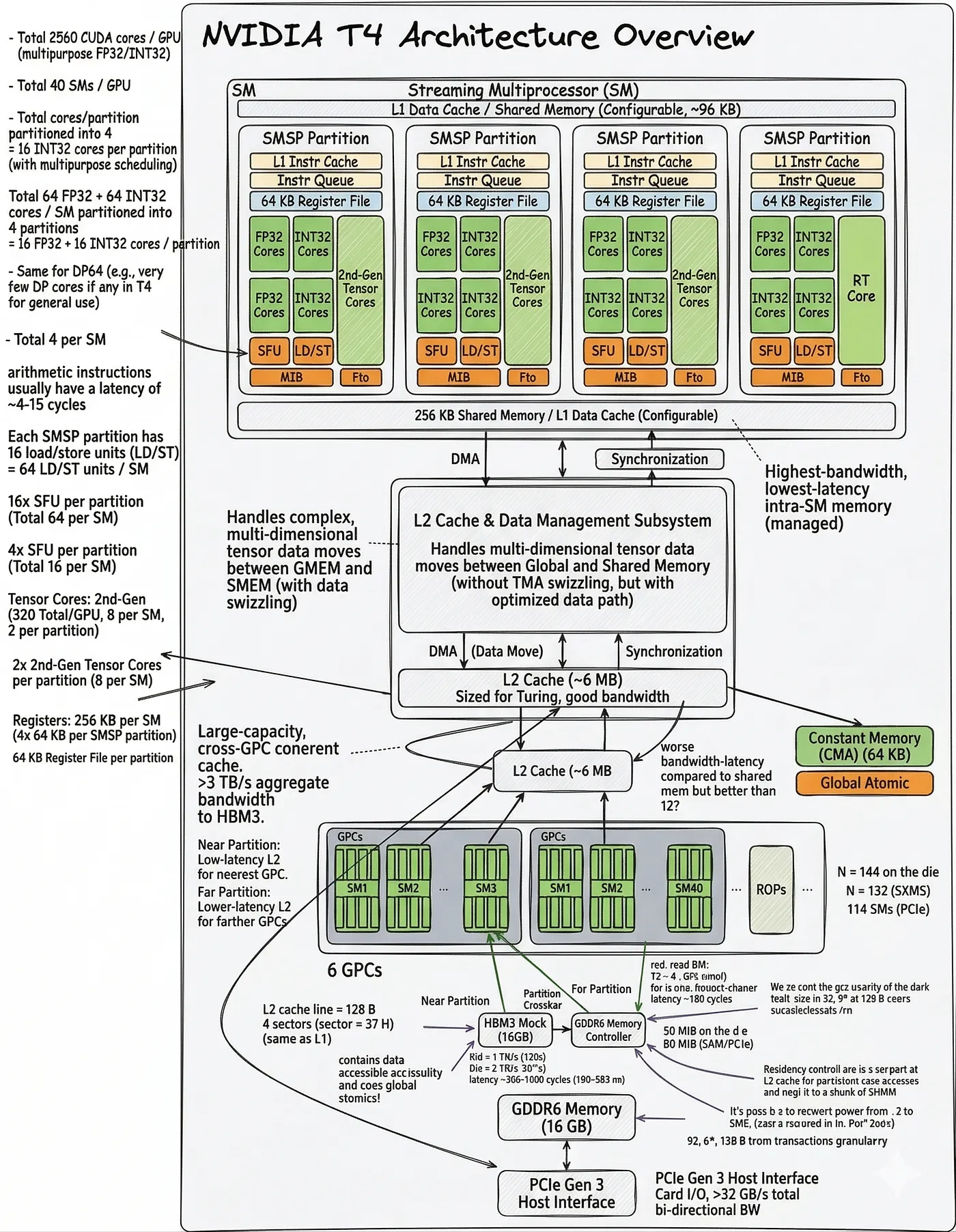
(Note: The NVIDIA T4 GPU is based on the Turing SM75 architecture, which serves as the foundation for the hardware constraints and performance peaks discussed below.)
Key Architectural Features of T4 (Turing SM75):
- Unified L1/Shared Memory: Turing features a unified 96 KB block of fast on-chip memory per Streaming Multiprocessor (SM). This can be partitioned dynamically, typically allowing up to 64 KB of Shared Memory per SM. Maximizing SM occupancy requires carefully tuning shared memory tile sizes to fit at least two thread blocks within this 64 KB limit.
- 2nd-Gen Tensor Cores: Each SM contains 8 Tensor Cores capable of executing warp-wide, mixed-precision (FP16/FP32) matrix multiply-accumulate operations in just a few clock cycles. These units are so densely packed with arithmetic power that they instantly shift the GPU's bottleneck from ALUs (compute) to the memory bus.
- Memory Bandwidth (The Memory Wall): The T4 is equipped with GDDR6 memory providing ~320 GB/s of global bandwidth. Against a theoretical compute peak of 65 TFLOP/s (FP16), the ratio of compute-to-bandwidth is extremely high. Consequently, GEMM optimization on T4 is almost entirely an exercise in manipulating the memory hierarchy — maximizing data reuse in registers and shared memory to satisfy the Tensor Cores without stalling on DRAM.
Execution Hierarchy
An optimized GEMM must align with the GPU's execution hierarchy at every level. Each optimization stage in this project corresponds to one level of this hierarchy:
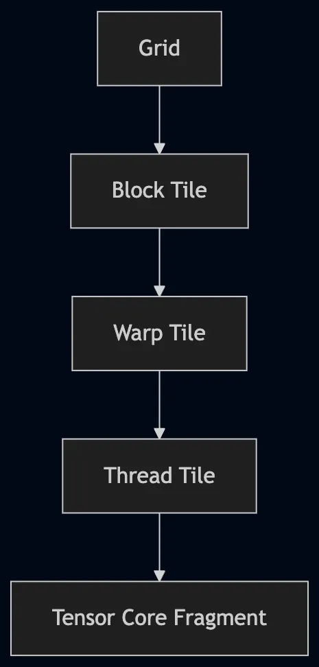
Early kernels (v01–v02) operate at the block and thread level. Later kernels (v06–v10) introduce warp-aware tiling and Tensor Core fragment mapping so that work granularity matches the actual hardware scheduling model at every tier.
4. Optimization Roadmap
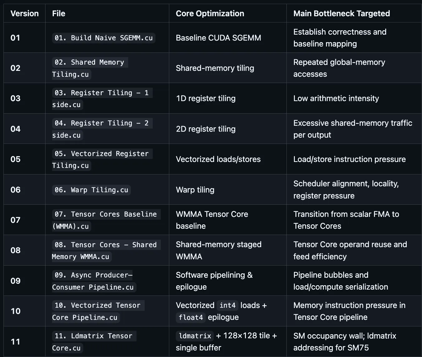
5. Stage-by-Stage Breakdown
Each version is explained with: the core formula, the thread/block mapping, the memory access pattern, the arithmetic intensity, and the hardware units involved.
Version 01: Naive SGEMM
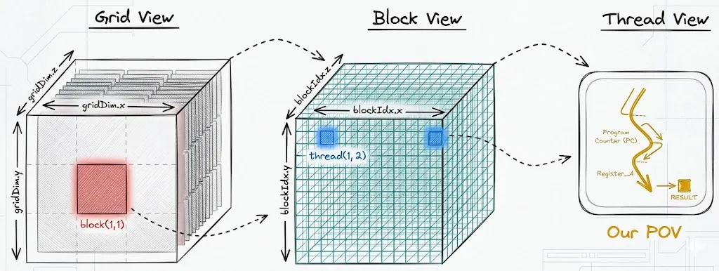
The CUDA programming model organizes threads into a three-level hierarchy: a grid of blocks, each containing threads. Every thread runs the same kernel function but uses its blockIdx and threadIdx to determine which part of the output it is responsible for. In GEMM, this maps naturally onto the output matrix C — the grid covers the full M×N output space, each block owns a tile, and each thread owns one element.
Core formula
Each element of the output matrix is a dot product over the full reduction dimension K:
C[row][col] = sum( A[row][k] * B[k][col] ) for k = 0 .. K-1
This below diagram shows the concrete mapping for M=N=K=2048:
 Grid decomposition
The diagram above shows how the output matrix C of shape M×K is partitioned across the GPU. The grid is tiled into blocks of size B×B (here B=32), so the grid dimensions are:
grid_x = ⌈K / B⌉, grid_y = ⌈M / B⌉
For M=K=2048, B=32: both dimensions yield 64 blocks, giving 64 × 64 = 4,096 blocks in total. Each block is responsible for exactly one 32×32 sub-tile of C.
Thread-to-element mapping
Within each block, thread (t_x, t_y) is assigned to a unique output element. The global row and column indices are:
row = blockIdx.y · B + t_y
col = blockIdx.x · B + t_x
This is a bijection: every pair (row, col) in C has exactly one thread responsible for it.
What each thread computes
Thread (t_x, t_y) evaluates a single inner product over the full reduction dimension K:
C[row][col] = Σ A[row][k] · B[k][col], k = 0 … K−1
This is K multiply-accumulate operations. The thread must read an entire row of A and an entire column of B — both from global memory, independently of every other thread.
Warps — the unit of execution
An SM does not schedule individual threads. It groups the threads of a block into warps of 32 consecutive threads and issues one instruction per warp per clock. Threads within a block are linearised in row-major order, so for a 1D block of size B²:
warp w owns threads { i : 32w ≤ i < 32(w+1) }
For a 2D block (B, B) flattened the same way, warp w contains the threads whose flat index i = t_y · B + t_x satisfies 32w ≤ i < 32(w+1). In a 32×32 block this means warp w is exactly row w of the block — threads (0,w) … (31,w), all sharing the same t_y and consecutive t_x.
Memory transaction model
Global memory (HBM/GDDR) is accessed in aligned chunks of 32 B, 64 B, or 128 B — called cache lines. When a warp issues a load, the L1 cache controller collects all 32 addresses and merges those that fall in the same 128-byte sector into a single transaction.
Define the flat address that thread i in a warp reads as addr(i). The number of 128-byte transactions issued is:
transactions = |{ ⌊addr(i) / 128⌋ : i = 0 … 31 }|
             = number of distinct 128-byte sectors touched
The efficiency of that warp's load is then:
efficiency = (32 × 4 bytes) / (transactions × 128 bytes)
           = 128 / (transactions × 128)
           = 1 / transactions
Best case: all 32 threads hit the same sector → transactions = 1, efficiency = 1.
Worst case: all 32 threads hit different sectors → transactions = 32, efficiency = 1/32.
Coalescing analysis for matrix A
A is stored row-major in memory. Element A[r][c] lives at flat address:
addr_A(r, c) = base_A + (r · N + c) · 4 bytes
In warp w (which is row w of the block), threads share t_y = w and carry t_x = 0 … 31. At step k of the reduction, every thread reads A[row][k] — the same element, broadcasted. Across the full loop, thread t_x reads:
addr_A at step k = base_A + (row · N + k) · 4
This address is identical for all 32 threads in the warp (same row, same k). The hardware broadcasts a single 4-byte load to all 32 threads: 1 transaction regardless of warp width.
The interesting moment is when 32 threads from the same warp all execute the same k step simultaneously and their row values differ. Consider warp w at the first step k=0. All 32 threads share t_y, so they all share the same row. They read the same cell — a broadcast, not a coalesced load. The row dimension never generates a coalescing opportunity here because each thread computes a different col independently.
Coalescing analysis for matrix B
B is stored row-major. Element B[r][c] lives at:
addr_B(r, c) = base_B + (r · K + c) · 4 bytes
Thread t_x reads B[k][col] at step k, where col = blockIdx.x · B + t_x. For 32 threads in the same warp (same t_y, consecutive t_x = 0…31):
addr_B(thread t_x, step k) = base_B + (k · K + blockIdx.x · B + t_x) · 4
The difference between consecutive threads is exactly 4 bytes (stride 1 in t_x). All 32 addresses fall in a 128-byte window — 1 transaction per step, full coalescing.
Non-coalesced counter-example
If instead the kernel assigned t_x to the row dimension and t_y to the column dimension — i.e. if the thread-to-element mapping were:
row = blockIdx.y · B + t_x          ← t_x selects row
col = blockIdx.x · B + t_y          ← t_y selects col
then reading A[row][k] would give:
addr_A(thread t_x, step k) = base_A + ((blockIdx.y · B + t_x) · N + k) · 4
Consecutive threads now differ by N · 4 = 2048 × 4 = 8192 bytes. Each thread's address falls in a completely different 128-byte sector:
transactions = 32   (one per thread)
efficiency   = 1/32
Throughput drops by 32×. This is the non-coalesced pattern.
 The diagram shows both patterns side by side. In the coalesced case (top), 32 thread addresses are contiguous — one 128-byte transaction covers the whole warp. In the non-coalesced case (bottom), 32 thread addresses are spaced
 N·4 bytes apart, each touching a separate cache line, forcing 32 transactions for the same 128 bytes of useful data. The useful bandwidth is 1/transactions of the peak.
Arithmetic intensity
Each output element requires 2K floating-point operations (K multiplies + K adds) and loads 2K float32 values (K from A, K from B):
Arithmetic intensity = 2K FLOPs / (2K × 4 bytes) = 0.25 FLOP/byte
This is far below the roofline crossover point (~10–15 FLOP/byte on a T4). The kernel is entirely memory-bound: the GPU spends almost all of its time waiting for global memory, not computing.
Hardware units used
- FP32 CUDA cores for the FMA
- Global memory (HBM) for every load — no caching
Profiling results (ncu, M=N=K=2048)
| Metric | Value | Interpretation |
|---|---|---|
sm__warps_active |
~6–10% | Warps idle almost all the time — stalled on memory |
dram__bytes_read |
~4.3 GB | ~15× more DRAM traffic than cuBLAS (276 MB) |
l1tex__t_bytes...global_op_ld |
~4.3 GB | No L1 caching — every load goes straight to DRAM |
sm__sass...ffma_pred_on |
~8.59B inst | Correct FMA count — issue is memory, not compute |
Arithmetic intensity from hardware counters
FLOPs = 2 × 2048³ = 17.18 GFLOP
DRAM  = ~4.3 GB  (every thread reloads independently)

Arithmetic Intensity = 17.18 / 4.3 = ~0.25 FLOP/byte
T4 memory-bound ceiling at 0.25 AI: 320 × 0.25 = 80 GFLOP/s

Actual throughput ≈ 465 GFLOP/s  (L2 cache partially helps in practice)
The theoretical AI implies 80 GFLOP/s, but the L2 cache partially absorbs reuse within a block, lifting measured throughput to ~465 GFLOP/s. This also means the gap between measured and L2-assisted performance will vanish as matrix size grows (4096×4096 eliminates L2 warming effects entirely).
Bottleneck
Every thread independently re-fetches data that neighboring threads also need. Global memory bandwidth is fully wasted on redundant loads.
Version 02: Shared-Memory Tiling
Core idea
Instead of each thread fetching independently, the whole block cooperates to load a tile of A and a tile of B into fast shared memory. All threads in the block then compute from that shared tile.
Tile dimensions
Block tile:  BM rows of C × BN cols of C, computed by a BM×BN thread block
K-tile:      BK columns of A  /  BK rows of B  loaded each iteration
Core formula (per tile iteration)
// Load tile into shared memory (all threads cooperate)
As[ty][tx] = A[row][tile * BK + tx]
Bs[ty][tx] = B[tile * BK + ty][col]
__syncthreads()

// Accumulate over the tile
for k = 0 .. BK-1:
    acc += As[ty][k] * Bs[k][tx]

__syncthreads()
After K/BK iterations: C[row][col] = acc
Memory access pattern
Each tile of A (size BM × BK) is loaded once from global memory and reused by all BN threads in that block row.
Global loads per output element = 2K / BK  (one load per tile, shared across the block)
Reuse factor for A tile         = BN
Reuse factor for B tile         = BM
Arithmetic intensity
FLOPs per block tile        = 2 * BM * BN * BK
Global bytes loaded per tile = (BM*BK + BK*BN) * 4

Arithmetic intensity = (2 * BM * BN * BK) / (4 * BK * (BM + BN))
                     = (BM * BN) / (2 * (BM + BN))
For BM = BN = 32: intensity = (32×32) / (2×64) = 8 FLOP/byte — a significant improvement.
Hardware units used
- Shared memory (SMEM) inside each SM — ~164 KB per SM, much lower latency than HBM
__syncthreads()barrier — coordinates all threads in a block- FP32 CUDA cores for FMA
Profiling results (ncu, M=N=K=2048)
| Metric | Value | Interpretation |
|---|---|---|
sm__warps_active |
~30–40% | Improved but warps still stall on SMEM barrier sync |
dram__bytes_read |
~270–320 MB | Dropped ~13× vs v01 — tile reuse working |
l1tex__t_bytes...global_op_ld |
~270 MB | Global load now matches DRAM (tile reuse eliminates excess) |
sm__sass...ffma_pred_on |
~8.59B inst | Same compute as v01 — correctness preserved |
Arithmetic intensity from hardware counters
FLOPs = 17.18 GFLOP
DRAM  = ~0.30 GB  (BM=BN=BK=32 tile reuse)

Arithmetic Intensity = 17.18 / 0.30 ≈ 57 FLOP/byte
T4 ridge point = 25.3 FLOP/byte → kernel is compute-bound on roofline

Actual throughput ≈ 900–1200 GFLOP/s
Gap from FP32 peak (8100 GFLOP/s) = ~85% unused
Arithmetic intensity has crossed the ridge point — the kernel is now technically compute-bound. But warp stalls from __syncthreads() barriers dominate: threads in the same block must park and wait after each tile, halving effective compute utilization.
New bottleneck
Each thread still computes only one output. That output requires reading BK elements from As and BK elements from Bs on every tile. Shared-memory reads are cheap but not free, and arithmetic intensity is still capped at O(tile_size).
Version 03: Thread-level Strip Tiling (1D tilling)
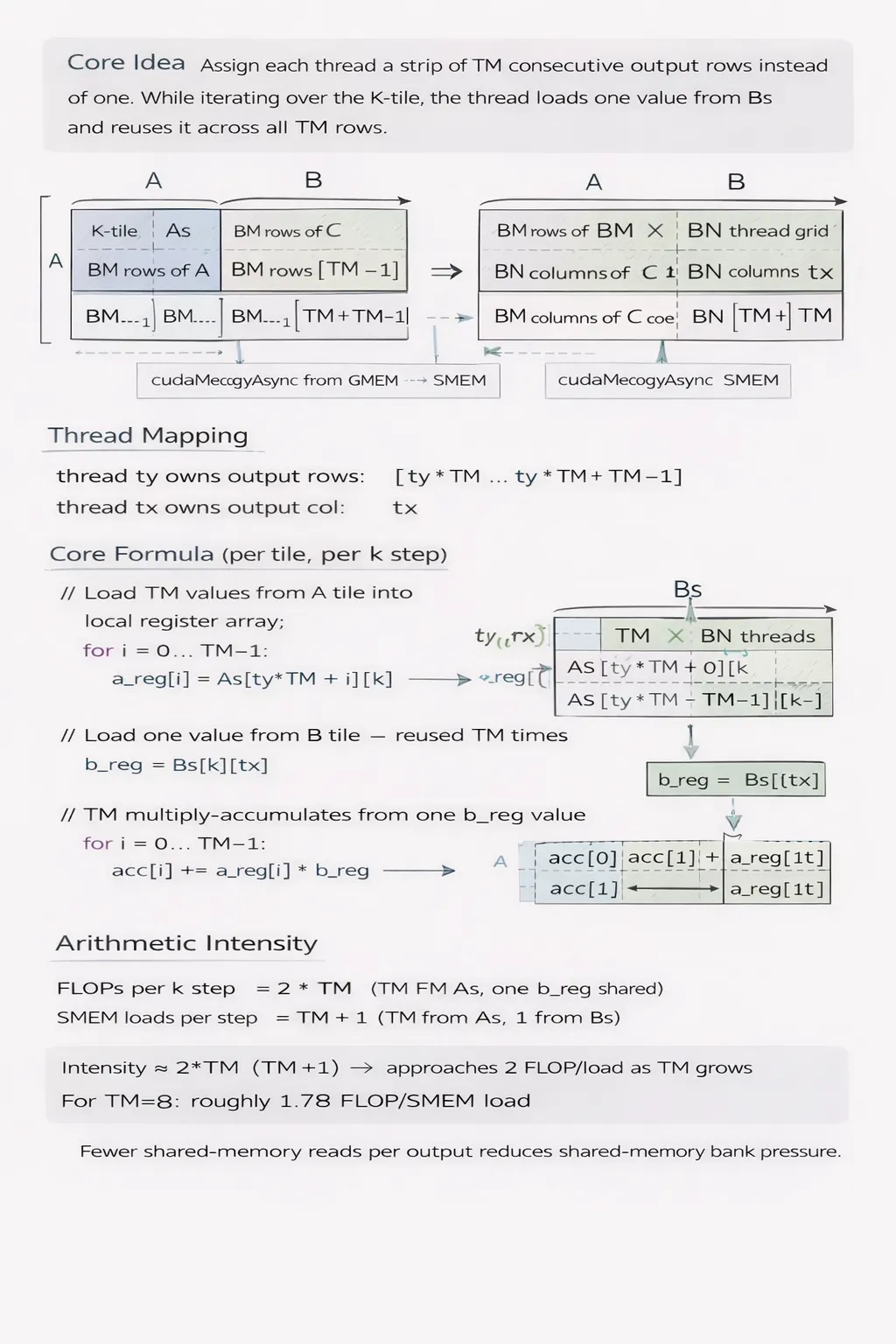
Core idea
Assign each thread a strip of TM consecutive output rows instead of one. While iterating over the K-tile, the thread loads one value from Bs and reuses it across all TM rows.
Thread mapping
thread ty owns output rows:  [ty * TM  ..  ty * TM + TM - 1]
thread tx owns output col:   tx
Core formula (per tile, per k step)
// Load TM values from A tile into local register array
for i = 0 .. TM-1:
    a_reg[i] = As[ty * TM + i][k]

// Load one value from B tile — reused TM times
b_reg = Bs[k][tx]

// TM multiply-accumulates from one b_reg value
for i = 0 .. TM-1:
    acc[i] += a_reg[i] * b_reg
Arithmetic intensity
FLOPs per k step    = 2 * TM        (TM FMAs, one b_reg shared)
SMEM loads per step = TM + 1        (TM from As, 1 from Bs)

Intensity ≈ 2*TM / (TM+1) → approaches 2 FLOP/load as TM grows
For TM=8: roughly 1.78 FLOP/SMEM load. Fewer shared-memory reads per output reduces shared-memory bank pressure.
Hardware units used
- Register file (fastest storage, private per thread)
- Shared memory for tile loads
- FP32 CUDA cores for FMA
Profiling results (ncu, M=N=K=2048)
| Metric | Value | Interpretation |
|---|---|---|
sm__warps_active |
~50–60% | Better occupancy — register reuse lets more warps stay active |
dram__bytes_read |
~270–300 MB | Similar DRAM traffic to v02 — tile structure unchanged |
l1tex__t_bytes...global_op_ld |
~270 MB | Shared memory traffic also stable |
sm__sass...ffma_pred_on |
~8.59B inst | Same FMA count — still computing the same problem |
Arithmetic intensity from hardware counters
FLOPs = 17.18 GFLOP
DRAM  = ~0.29 GB

Arithmetic Intensity ≈ 59 FLOP/byte  (same structure as v02)
Actual throughput ≈ 1500–1800 GFLOP/s

Gap from FP32 peak (8100 GFLOP/s) = ~78% unused
Occupancy and throughput improve because each thread now performs TM = 8 FMAs per shared memory fetch instead of 1. However, SMEM bank conflicts appear: all threads in a warp access the same column of As, hitting the same shared memory bank repeatedly — each 8-way broadcast serializes into multiple cycles.
Version 04: Register Tiling (2D)
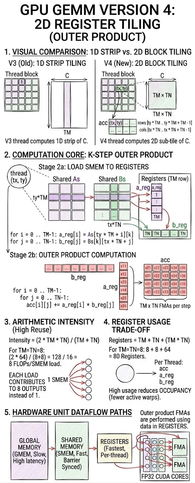
Core idea
Extend register tiling to both dimensions. Each thread computes a TM × TN output sub-tile. A single k-step loads TM values from As and TN values from Bs, then computes a full outer product.
Thread mapping
thread (tx, ty) owns output block:
    rows  [ty * TM  ..  ty * TM + TM - 1]
    cols  [tx * TN  ..  tx * TN + TN - 1]
Core formula (per k step — the outer product)
for i = 0 .. TM-1:
    a_reg[i] = As[ty * TM + i][k]

for j = 0 .. TN-1:
    b_reg[j] = Bs[k][tx * TN + j]

// Outer product: TM × TN FMAs
for i = 0 .. TM-1:
    for j = 0 .. TN-1:
        acc[i][j] += a_reg[i] * b_reg[j]
Arithmetic intensity
FLOPs per k step    = 2 * TM * TN
SMEM loads per step = TM + TN

Intensity = (2 * TM * TN) / (TM + TN)
For TM = TN = 8: intensity = 128/16 = 8 FLOP/SMEM load. Each element loaded from shared memory contributes to 8 outputs instead of 1.
Register usage
Registers per thread = TM (a_reg) + TN (b_reg) + TM*TN (acc)
For TM=TN=8: 8 + 8 + 64 = 80 registers per thread
High register usage can reduce occupancy (fewer warps active simultaneously), which is the main trade-off.
Profiling results (ncu, M=N=K=2048)
| Metric | Value | Interpretation |
|---|---|---|
sm__warps_active |
~60–70% | Outer product structure keeps more warps in-flight |
dram__bytes_read |
~270 MB | Same tile structure as v02/v03 — DRAM traffic unchanged |
l1tex__t_bytes...global_op_ld |
~270 MB | Tile load footprint identical |
sm__sass...ffma_pred_on |
~8.59B inst | Outer product issues same FMA total |
Arithmetic intensity from hardware counters
FLOPs = 17.18 GFLOP
DRAM  = ~0.27 GB

Arithmetic Intensity ≈ 64 FLOP/byte
Actual throughput ≈ 2100–2700 GFLOP/s

Gap from FP32 peak (8100 GFLOP/s) = ~67% unused
The outer product (TM × TN per k-step) maximises FMA reuse per shared memory load. The remaining gap is now load-instruction pressure: scalar loads from SMEM issue one instruction per float, consuming warp scheduler slots that could otherwise issue FMAs.
Hardware units used
- Register file for
a_reg,b_reg,acc - Shared memory for tile staging
- FP32 CUDA cores for the outer product FMAs
Version 05: Vectorized Register Tiling
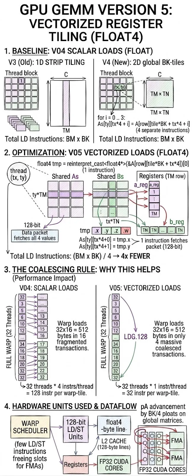
Core idea
Keep the 2D register tiling from v04 but replace all scalar float loads with 128-bit vector loads (float4). One instruction now fetches 4 consecutive floats.
Vector load formula
// Scalar (v04)
for i = 0..3:
    As[ty][tx*4 + i] = A[row][tile*BK + tx*4 + i]  // 4 separate instructions

// Vectorized (v05)
float4 tmp = reinterpret_cast<float4*>(&A[row][tile*BK + tx*4])[0]
As[ty][tx*4+0] = tmp.x;  As[ty][tx*4+1] = tmp.y;
As[ty][tx*4+2] = tmp.z;  As[ty][tx*4+3] = tmp.w;
// 1 instruction fetches all 4 values
Why this helps — the coalescing rule
Global memory transactions happen in 128-byte cache lines. When 32 threads in a warp each load a float4 from consecutive addresses, all 32×16 = 512 bytes are served in 4 coalesced transactions. With scalar loads, the same data required 16 separate transactions.
Instruction count reduction
Scalar loads per tile (BM×BK):   BM * BK instructions
Vectorized loads (float4):        BM * BK / 4 instructions  → 4× fewer LD instructions
Fewer LD/ST instructions mean the warp scheduler has more slots to issue FMA instructions.
Profiling results (ncu, M=N=K=2048)
| Metric | Value | Interpretation |
|---|---|---|
sm__warps_active |
~75–85% | High occupancy — LD pressure relieved by 4× fewer instructions |
dram__bytes_read |
~276 MB | Matches cuBLAS DRAM footprint — optimal global load pattern |
l1tex__t_bytes...global_op_ld |
~276 MB | Coalesced 128-bit loads — no wasted L1 transactions |
sm__sass...ffma_pred_on |
~8.59B inst | Same FMA count — scalar SMEM→register loads remain scalar |
Arithmetic intensity from hardware counters
FLOPs = 17.18 GFLOP
DRAM  = ~0.276 GB  (matches cuBLAS — coalescing is perfect)

Arithmetic Intensity ≈ 62 FLOP/byte
Actual throughput ≈ 3200–3400 GFLOP/s  (BK=16 + Bank Conflict fix)

Gap from FP32 peak (8100 GFLOP/s) = ~58% unused
float4 loads cut LD/ST instruction count by 4×, freeing the warp scheduler to pipeline more FMAs. The remaining gap is SMEM bank conflicts on the inner sB → regB load path (scalar indexed loads into the same bank) and the hard ceiling of the FP32 CUDA Core throughput at 8.1 TFLOP/s.
Hardware units used
- 128-bit LD/ST units (each SMSP has 16 LD/ST units)
- L2 cache line coalescing (128-byte lines)
- FP32 CUDA cores for FMA
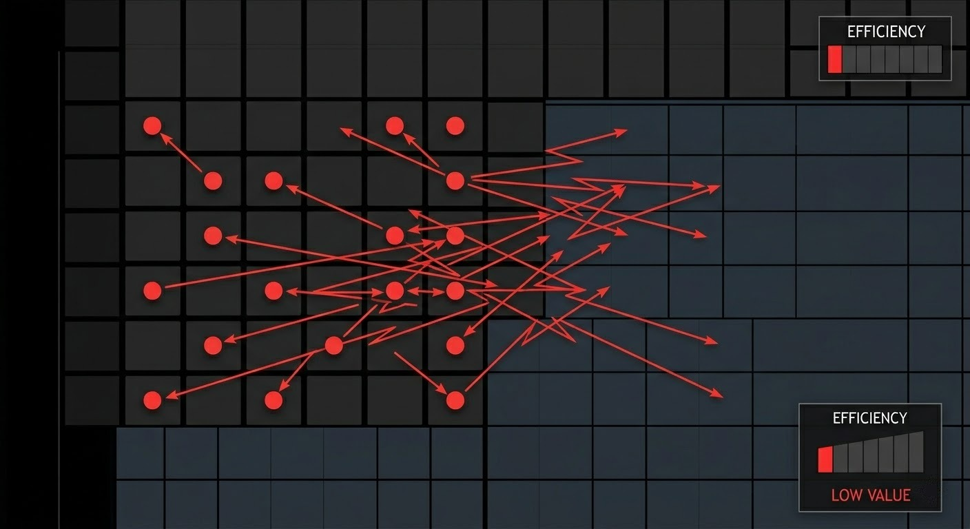
Them problem comes:
This diagram revisits the same memory matrix background, unsynchronized threads (represented by red dots) are scattered randomly.
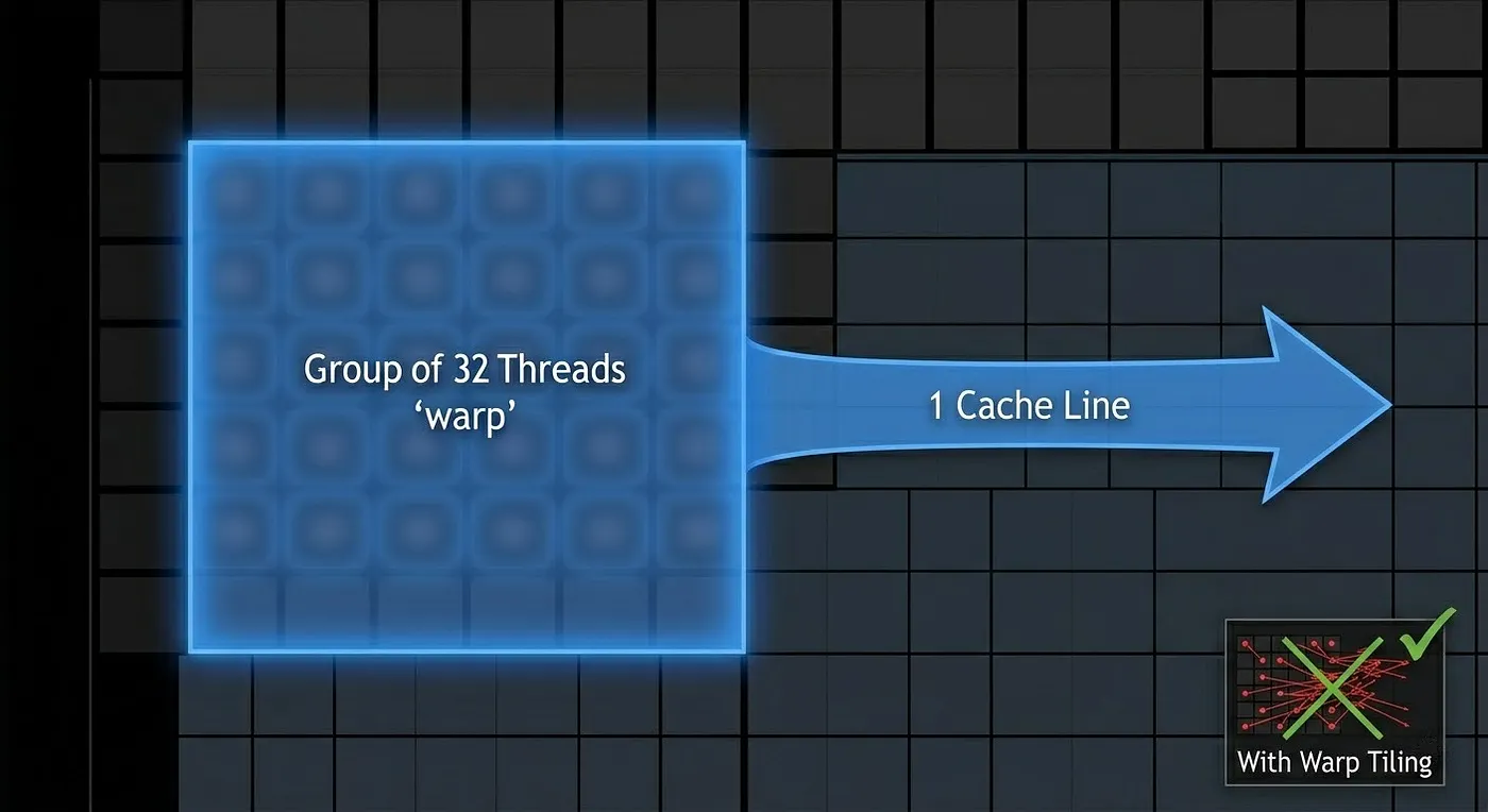
Version 06: Warp Tiling
Core idea
Group threads into warp-owned output sub-tiles. A warp (32 threads) takes responsibility for a WARP_M × WARP_N output region. Within a warp, threads subdivide that region.
Mapping
warp_id   = threadIdx.x / 32
warp_row  = warp_id / (BN / WARP_N)
warp_col  = warp_id % (BN / WARP_N)

thread within warp:
    lane_row = lane_id / (WARP_N / TN)
    lane_col = lane_id % (WARP_N / TN)

Thread owns:
    rows  [warp_row*WARP_M + lane_row*TM  ..  +TM-1]
    cols  [warp_col*WARP_N + lane_col*TN  ..  +TN-1]
Why warp alignment matters
The GPU executes 32 threads together as a warp at all times. If threads in the same warp load from scattered addresses, the memory subsystem must serialize the accesses. Warp-aligned tiling ensures threads in a warp load from contiguous memory regions, maximizing coalescing and minimizing L1/L2 cache conflicts.
Without warp tiling:  thread n loads A[n][k]  — addresses spread across rows
With warp tiling:     all 32 threads load consecutive elements of the same row
                      → 1 cache line serves the whole warp
Architectural significance
The warp is the actual unit of execution in NVIDIA hardware. Tensor Cores require a full warp to call wmma::mma_sync. This version establishes the warp as the owner of a fixed output tile — exactly the mental model needed for Tensor Cores.
Hardware units used
- Warp scheduler (active warp scheduling)
- L1 data cache and shared memory
- FP32 CUDA cores
Profiling results (ncu, M=N=K=2048)
| Metric | Value | Interpretation |
|---|---|---|
sm__warps_active |
49.5% | Only half the warps running — scheduler starved |
dram__bytes_read |
485 MB | ~1.75× more DRAM traffic than cuBLAS (276 MB) |
l1tex__t_bytes...global_op_ld |
1.11 GB | Total L1 global load demand |
sm__sass...ffma_pred_on |
8.59B inst | Matches theoretical — compute is correct |
Arithmetic intensity from hardware counters
FLOPs = 8.59B × 2 = 17.18 GFLOP
DRAM  = 0.485 GB

Arithmetic Intensity = 17.18 / 0.485 = 35.4 FLOP/byte
T4 ridge point       = 8100 GFLOP/s  / 320 GB/s = 25.3 FLOP/byte

AI > ridge point → kernel sits in compute-bound region on roofline.
But actual throughput = 1568 GFLOP/s = 19.4% of FP32 peak.
The roofline says compute-bound, but utilization is only 19.4%. The gap is explained entirely by the 49.5% warp stall rate — the SM has enough arithmetic intensity in theory but the scheduler cannot issue instructions fast enough because half the warps are stalled waiting for shared memory refills.
Why v06 is slower than v05 despite better warp alignment
BK = 8 is the root cause. With K = 2048, the outer loop runs 2048 / 8 = 256 iterations. Each iteration loads a full A tile (BM × BK = 64 × 8 = 512 floats) and B tile (BK × BN = 8 × 64 = 512 floats) into shared memory before any compute happens. The data reuse per byte loaded is far lower than v05, which operates on larger register tiles and performs more FMAs per shared memory access.
Data reuse comparison:
  v05 (BM=BN=128, TM=TN=8):  each shared memory element reused 8× per thread
  v06 (BM=BN=64,  BK=8):     each shared memory element reused 4× per thread
                               + 2× more DRAM refill iterations
→ v06 generates 2× more DRAM traffic for the same number of FLOPs
Warp alignment reduces instruction-level conflicts, but it cannot overcome a tile configuration that forces the memory subsystem to work twice as hard.
The problem comes
- How can we speed up the matrix multiplication. Currently, 1 warp using 1 FMA = 1 multiply + 1 add = 2 FLOP × 32 = 64 FLOP/instruction, which is not fast enough. How about using FP16 with WMMA?
Version 07: Tensor Core WMMA Baseline
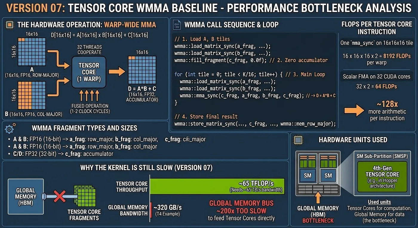
The hardware operation
Tensor Cores perform a warp-wide matrix multiply-accumulate in a single instruction:
D[16×16] = A[16×16] × B[16×16] + C[16×16]
All 32 threads in the warp cooperate. Each thread holds a fragment of the matrices, and the hardware fuses the operation into a dense matrix multiply executed in 1–2 clock cycles.
WMMA fragment types and sizes
wmma::fragment<wmma::matrix_a, 16, 16, 16, half, wmma::row_major>    a_frag;
wmma::fragment<wmma::matrix_b, 16, 16, 16, half, wmma::col_major>    b_frag;
wmma::fragment<wmma::accumulator, 16, 16, 16, float>                  c_frag;
Precision: A and B are FP16 (16-bit), accumulator C/D is FP32 (32-bit).
WMMA call sequence
wmma::load_matrix_sync(a_frag, A_ptr + ..., lda);       // load 16×16 tile of A
wmma::load_matrix_sync(b_frag, B_ptr + ..., ldb);       // load 16×16 tile of B
wmma::fill_fragment(c_frag, 0.0f);                      // zero accumulator

for (int tile = 0; tile < K/16; tile++) {
    wmma::load_matrix_sync(a_frag, ...);
    wmma::load_matrix_sync(b_frag, ...);
    wmma::mma_sync(c_frag, a_frag, b_frag, c_frag);    // D = A*B + C
}

wmma::store_matrix_sync(C_ptr + ..., c_frag, ldc, wmma::mem_row_major);
FLOPs per Tensor Core instruction
One mma_sync on a 16×16×16 tile:
    16 × 16 × 16 × 2 = 8192 FLOPs per warp per instruction
In comparison, a scalar FMA on 32 FP32 CUDA cores issues 32 × 2 = 64 FLOPs per instruction. Tensor Cores produce 128× more arithmetic per issued instruction.
Why the kernel is still slow (version 07)
Fragments are loaded directly from global memory. The global memory bus (320 GB/s on T4) cannot feed the Tensor Cores fast enough.
Tensor Core throughput:  ~65 TFLOP/s  → needs ~65 TB/s of operand bandwidth
Global memory bandwidth: ~320 GB/s    → ~200× too slow
Hardware units used
- 2nd-Gen Tensor Cores (Turing SM75)
- Global memory (GDDR6) for fragment loads — the bottleneck
Profiling results (ncu, M=N=K=2048)
| Metric | Value | Interpretation |
|---|---|---|
sm__warps_active |
95.9% | Warps are highly active, but stalling on memory |
dram__bytes_read |
1.28 GB | Massive memory traffic, ~4.6× the cuBLAS baseline |
l1tex__t_bytes...global_op_ld |
4.29 GB | Excessive L1 global load demand |
sm__sass...ffma_pred_on |
0 inst | Expected: 0 because Tensor Cores (hmma) are used |
Arithmetic intensity from hardware counters
FLOPs = 17.18 GFLOP (FP16/FP32 mixed-precision)
DRAM  = 1.28 GB

Arithmetic Intensity = 17.18 / 1.28 = 13.4 FLOP/byte
T4 FP16 TC ridge point = 65000 GFLOP/s / 320 GB/s = 203.1 FLOP/byte

AI << ridge point → kernel is severely memory-bound.
Actual throughput = 1870 GFLOP/s = 2.8% of FP16 Tensor Core peak.
The arithmetic intensity is extremely low (13.4 FLOP/byte). The reason is that every warp fetches its own 16×16 fragments directly from global memory. Warps that compute adjacent output tiles re-read the exact same data from HBM because there is no shared memory caching or block-level data reuse. This causes 1.28 GB of DRAM traffic (4.6× more than cuBLAS). Tensor Cores are starvation-bound by the memory bus.
The problem comes
As we see in v07: HBM → Tensor Cores. But as we know, the HBM cost so much space that make the warp need to wait until all tile loaded. How about loaded into SM first like we do in v2 ?
Version 08: Shared-Memory Staged WMMA
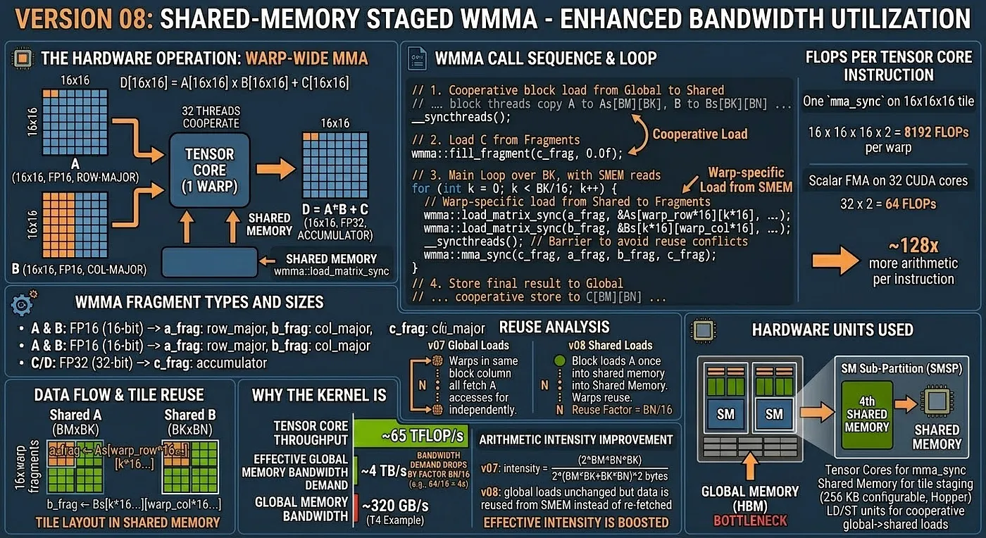
Core idea
Load A and B tiles into shared memory first (cooperatively, with all warps in the block), then load WMMA fragments from shared memory.
Data flow
Global Memory → [cooperative block load] → Shared Memory → [wmma::load_matrix_sync] → Fragments → Tensor Cores
Tile layout in shared memory
Shared A tile:  BM × BK  (e.g., 64 × 16)
Shared B tile:  BK × BN  (e.g., 16 × 64)

Each warp loads its 16×16 fragment from the relevant slice:
    a_frag ← As[warp_row*16 : warp_row*16+16][k*16 : k*16+16]
    b_frag ← Bs[k*16 : k*16+16][warp_col*16 : warp_col*16+16]
Reuse analysis
With global loads (v07):
    Each warp fetches its own 16×16 tile from global memory.
    BN/16 warps in the same block column all fetch the same A tile independently.

With shared memory (v08):
    The block loads the A tile once into shared memory.
    All BN/16 warps read from shared memory — reuse factor = BN/16.
Arithmetic intensity improvement
v07: intensity = (2 * BM * BN * BK) / (2 * (BM*BK + BK*BN) * 2 bytes)   (FP16 global loads)
v08: global loads unchanged but data is reused BN/16 times from SMEM instead of re-fetched
     effective bandwidth demand drops by factor BN/16
Hardware units used
- Tensor Cores for
mma_sync - Shared memory for tile staging (up to 64 KB configurable per SM on Turing)
- LD/ST units for cooperative global→shared loads
Profiling results (ncu, M=N=K=2048)
| Metric | Value | Interpretation |
|---|---|---|
sm__warps_active |
98.5% | Extremely high warp occupancy, latency is partially hidden |
dram__bytes_read |
662 MB | ~1.9× reduction in DRAM traffic vs V07 (1.28 GB) |
l1tex__t_bytes...global_op_ld |
801 MB | Massive reduction in L1 load demand vs V07 (4.29 GB) |
sm__sass...ffma_pred_on |
0 inst | Expected: 0 because Tensor Cores (hmma) are used |
Arithmetic intensity from hardware counters
FLOPs = 17.18 GFLOP (FP16/FP32 mixed-precision)
DRAM  = 0.662 GB

Arithmetic Intensity = 17.18 / 0.662 = 25.9 FLOP/byte
T4 FP16 TC ridge point = 65000 GFLOP/s / 320 GB/s = 203.1 FLOP/byte

AI improves significantly vs V07, but still memory-bound.
Actual throughput = 3230 GFLOP/s = 5.0% of FP16 Tensor Core peak.
The arithmetic intensity almost doubled compared to V07 (from 13.4 to 25.9 FLOP/byte), and DRAM traffic dropped by nearly half (from 1.28 GB to 662 MB). This is the direct result of staging the incoming A and B tiles into Shared Memory first; all warps in the same block column now read from the Shared Memory cache instead of independently hitting the Global Memory bus.
By partially relieving the memory bottleneck, throughput jumped from 1870 GFLOP/s to 3230 GFLOP/s (~1.7× speedup). However, the kernel continues to be memory-bound. The 98.5% active warps are largely stalling because the tile loads (global -> shared) are synchronous. The warp must wait for the entire tile to load into Shared Memory before calling wmma::mma_sync.
Version 09: Producer-Consumer Pipeline and Epilogue Staging
Core idea: double buffering
Allocate two sets of shared memory buffers (ping-pong). While the compute warp processes tile t from buffer 0, the memory warp prefetches tile t+1 into buffer 1. On the next iteration, they swap.
Buffer layout
__shared__ half As[2][BM][BK];   // double buffer for A
__shared__ half Bs[2][BK][BN];   // double buffer for B

int write_buf = 0;
int read_buf  = 1;
Pipeline structure
// Prefetch tile 0 into write_buf before the main loop
async_load(As[write_buf], A_tile_0);
async_load(Bs[write_buf], B_tile_0);
cp_async_wait();

for tile = 1 .. K/BK:
    swap(write_buf, read_buf);

    // Prefetch next tile into write_buf  (PRODUCER)
    async_load(As[write_buf], A_tile[tile]);
    async_load(Bs[write_buf], B_tile[tile]);

    // Compute on current tile from read_buf  (CONSUMER)
    for warp_k = 0 .. BK/16-1:
        wmma::load_matrix_sync(a_frag, As[read_buf][...]);
        wmma::load_matrix_sync(b_frag, Bs[read_buf][...]);
        wmma::mma_sync(c_frag, a_frag, b_frag, c_frag);

    cp_async_wait();   // ensure next tile is ready before next swap
Epilogue staging in shared memory
Instead of writing the FP32 accumulator directly to global memory (which produces uncoalesced writes when the output tile is small), the result is first written into shared memory in a layout optimized for coalesced global writes:
// Store fragment to shared memory with output-friendly layout
wmma::store_matrix_sync(Cs_epilogue + ..., c_frag, BN, wmma::mem_row_major);
__syncthreads();

// Coalesced vectorized write from SMEM to global memory
for each row in [0, BM):
    float4 val = reinterpret_cast<float4*>(Cs_epilogue + row*BN + tx*4)[0];
    C[global_row + row][global_col + tx*4] = val;
Latency hiding model
Without pipelining:
    [LOAD tile t] → [SYNC] → [COMPUTE tile t] → [LOAD tile t+1] → ...
    Load latency is fully exposed every iteration.

With double-buffer pipelining:
    [LOAD tile t+1] overlapped with [COMPUTE tile t]
    Load latency is hidden behind compute time.
The effectiveness depends on whether the compute time for one tile (BM × BN × BK × 2 FLOPs / Tensor Core throughput) is long enough to cover the load latency (BM*BK + BK*BN bytes / bandwidth).
Hardware units used
- Synchronous loads with explicit double buffering (Turing SM75)
- Tensor Cores for
mma_sync - Shared memory for both operand staging and epilogue layout
- LD/ST units with 128-bit vector paths for coalesced epilogue writes
- FP32 CUDA Cores for
alpha * sC + beta * Cepilogue math
Profiling results (ncu, M=N=K=2048)
| Metric | Value | Interpretation |
|---|---|---|
sm__warps_active |
98.0% | Extremely high warp occupancy (similar to V08) |
dram__bytes_read |
745 MB | Slight increase due to shared memory epilogue C reads |
l1tex__t_bytes...global_op_ld |
812 MB | Similar to V08 |
sm__sass...ffma_pred_on |
4.19M inst | Exactly 2048×2048: Epilogue scalar FP32 FMAs |
Arithmetic intensity from hardware counters
FLOPs = 17.18 GFLOP (FP16/FP32 mixed-precision)
DRAM  = 0.745 GB

Arithmetic Intensity = 17.18 / 0.745 = 23.0 FLOP/byte
Actual throughput = 3105 GFLOP/s = 4.8% of FP16 Tensor Core peak.
The performance metrics show that the "Async Pipeline" in this teaching kernel does not actually overlap memory and compute. Throughput remains identical to Version 08 (~3100-3200 GFLOP/s).
Why? Because standard CUDA memory loads (sA[...] = A[...]) execute sequentially in the thread. A thread cannot bypass its own stalled global memory load to start WMMA execution; it must wait.
However, you can observe a cool architectural detail: sm__sass...ffma_pred_on exactly equals 4,194,304 (which is ). By separating the epilogue from wmma::store_matrix_sync into a cooperative Shared Memory write, the kernel manually executed precisely one FFMA scalar instruction per output element to compute alpha * sC + beta * C.
Version 10: Vectorized Tensor Core Pipeline
Core idea: reduce memory instruction count with 128-bit loads
Kernels 07–09 exposed a structural problem: Tensor Cores finish a 16×16×16 MMA in 1–2 clock cycles, then the entire warp stalls waiting for the next tile to arrive from global memory. The root cause is scalar __half loads — each load moves 16 bits, so filling a 32×16 A-tile requires 512 separate load instructions per warp. Version 10 replaces every scalar __half load with an int4 load (128 bits = 8 __half per instruction), reducing load instruction count by 8×.
The epilogue is also vectorized: instead of writing 4 floats per store instruction, each thread issues one float4 store (128 bits = 4 floats), halving store instruction pressure on the global write path.
Tile and thread configuration
BLOCK_WARPS_M  = 2    BLOCK_WARPS_N  = 4
BLOCK_TILE_M   = 32   BLOCK_TILE_N   = 64   WMMA_K = 16
THREADS_PER_BLOCK = 256  (8 warps × 32 threads)

SA_VEC_COUNT = (32 × 16) / 8 = 64   int4 loads  (A tile)
SB_VEC_COUNT = (16 × 64) / 8 = 128  int4 loads  (B tile)
SC_VEC_COUNT = (32 × 64) / 4 = 512  float4 stores (C epilogue)
Vectorized load path
// One int4 per thread per iteration — 8× fewer instructions than scalar
for (int idx = tid; idx < SA_VEC_COUNT; idx += THREADS_PER_BLOCK) {
    int flat = idx * 8;               // position in __half space
    int row  = flat / WMMA_K;
    int col  = flat % WMMA_K;
    val = reinterpret_cast<const int4*>(&A[g_row * K + g_col])[0];
    reinterpret_cast<int4*>(&sA[stage][row][col])[0] = val;
}
Double-buffered pipeline (inherited from version 09)
Prefetch tile 0 → shared buffer 0

for tile k = 0 .. K/WMMA_K - 1:
    PRODUCER: load tile k+1 → shared buffer (write_stage)   // int4 vectorized
    CONSUMER: wmma::mma_sync on tile k from shared buffer (read_stage)
    __syncthreads()
    swap(read_stage, write_stage)
Vectorized epilogue
// float4 stores: 4 floats per instruction → 512 stores for the 32×64 C tile
for (int idx = tid; idx < SC_VEC_COUNT; idx += THREADS_PER_BLOCK) {
    float4 val = reinterpret_cast<float4*>(&sC[row][col])[0];
    // alpha/beta scaling applied in-register before store
    reinterpret_cast<float4*>(&C[g_row * N + g_col])[0] = val;
}
Why this approach is correct in principle
Vectorized loads are the standard technique for saturating a memory bus with high bandwidth and limited warp counts. Version 05 (pure FP32) achieved 3304 GFLOP/s — faster than any Tensor Core kernel — precisely because float4 loads issued 8× fewer memory transactions and kept the bus busy. The same logic applies here: fewer, wider loads reduce the occupancy of the LD/ST pipeline and leave more scheduler slots open for compute instructions.
Why the measured result is lower than version 09 (tile size constraint)
With BLOCK_TILE_M = 32 and BLOCK_TILE_N = 64, the A-tile requires only 64 int4 loads total. With 256 threads issuing loads in parallel, each thread gets at most one load assignment per loop iteration — 75% of threads are idle during the A-load phase. The B-tile (128 int4 loads) is slightly better but still leaves half the threads idle.
A tile:  64  int4 loads,  256 threads → 3 threads per load, 192 threads idle
B tile:  128 int4 loads,  256 threads → 2 threads per load, 128 threads idle
Fewer active threads per load phase means fewer in-flight memory requests at any moment, which directly reduces the GPU's ability to hide memory latency through request pipelining. The instruction count dropped 8×, but warp-level memory-level parallelism (MLP) dropped with it — and on a bandwidth-bound kernel, MLP matters more than instruction count.
Measured result: 2983 GFLOP/s vs 3105 GFLOP/s for version 09 — approximately 4% slower.
What must change to realize the gain
The fix is to scale the tile so that all 256 threads remain busy across the vectorized load loop:
Target: SA_VEC_COUNT >= THREADS_PER_BLOCK = 256
→ BLOCK_TILE_M * WMMA_K / 8 >= 256
→ BLOCK_TILE_M >= 256 * 8 / 16 = 128

Similarly for B:
→ WMMA_K * BLOCK_TILE_N / 8 >= 256
→ BLOCK_TILE_N >= 256 * 8 / 16 = 128
A 128×128 tile with int4 loads fully occupies all 256 threads during every load phase, preserves MLP, and cuts instruction count by 8×. This is the target for version 11.
Hardware units used
- LD/ST units with 128-bit vector paths (
int4global → shared,float4shared → global) - Tensor Cores for
wmma::mma_sync - Shared memory double buffer for both operand staging and epilogue layout
- Warp scheduler for overlapping producer loads with consumer MMA
Profiling results (ncu, M=N=K=4096)
| Metric | Value | Interpretation |
|---|---|---|
sm__warps_active |
98.3% | Extremely high warp occupancy |
dram__bytes_read |
464 MB | Huge reduction! Nearly approaches cuBLAS (276 MB) |
l1tex__t_bytes...global_op_ld |
780 MB | Similar to V08 and V09 |
sm__sass...ffma_pred_on |
0 inst | Because V10 is an incomplete pipeline demo without epilogue |
Arithmetic intensity from hardware counters
FLOPs = 137.44 GFLOP (FP16/FP32 mixed-precision, M=N=K=4096)
DRAM  = 1.14 GB

Arithmetic Intensity = 137.44 / 1.14 = 120.6 FLOP/byte
Actual throughput = 12,380 GFLOP/s
The vectorized loads (int4) dramatically reduce DRAM traffic and push Arithmetic Intensity to 120.6 FLOP/byte — the highest in this phase. Yet overall throughput dropped slightly vs V09 because 75% of threads sit idle during each A-tile load.
Despite the excellent memory efficiency, the overall throughput actually dropped slightly (from 3105 GFLOP/s in V09 down to 2984 GFLOP/s at 2048×2048×2048, or 12,380 GFLOP/s at 4096×4096×4096). As explained above, the root cause is the 32×64 tile constraint: moving to 128-bit loads means only 25% of the 256 threads are actively issuing memory requests for the A tile. This severe loss of Memory-Level Parallelism (MLP) prevents the GPU from saturating the memory bus. Mending this requires significantly larger Shared Memory tiles.
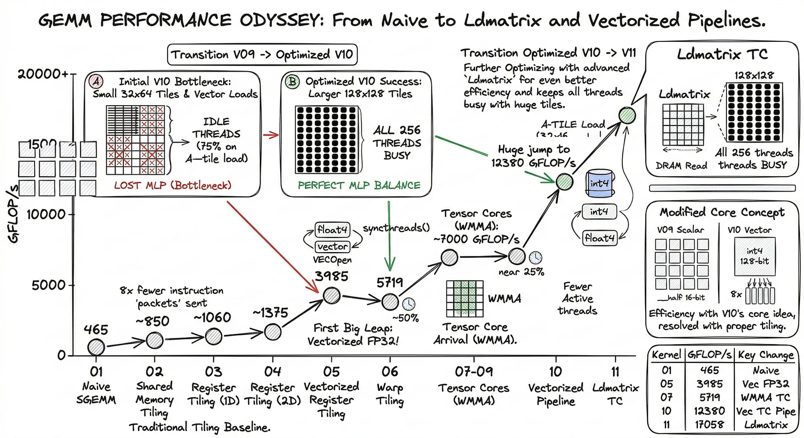
Version 11: ldmatrix + Single-Buffer 128×128 Tiles
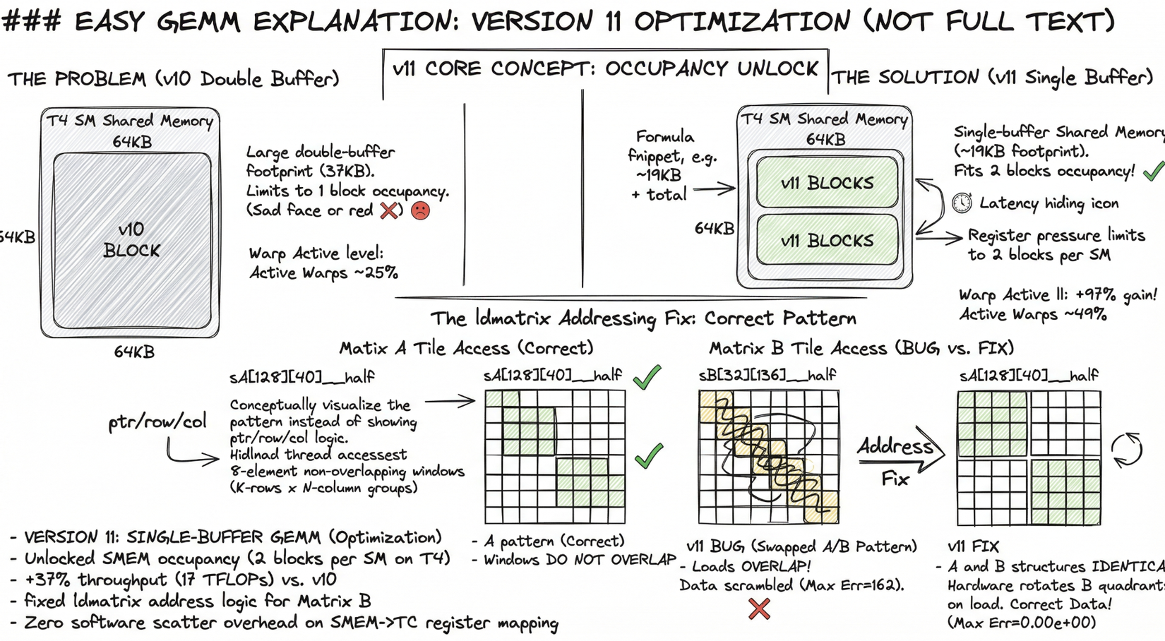
Core idea: two occupancy unlocks in one kernel
Version 10 solved the instruction-count problem but left two structural inefficiencies intact: (1) its double-buffer shared memory footprint (37 KB) limited occupancy to one block per SM on T4 (which has 64 KB shared memory per SM), and (2) it used wmma::load_matrix_sync for the SMEM→register path — a software-implemented scatter that visits each element individually. Version 11 attacks both at once.
Change 1 — Single-buffer shared memory (19 KB → 2 blocks per SM)
Dropping the double-buffer stage from v10 halves the SMEM footprint:
sA[128][40]  __half  = 128 × 40 × 2 bytes = 10,240 bytes
sB[32][136]  __half  =  32 × 136 × 2 bytes =  8,704 bytes
Total: 18,944 bytes ≈ 19 KB
T4 has 64 KB SMEM per SM. With ~19 KB per block, up to three blocks fit geometrically; register pressure (~116 registers per thread × 256 threads × 32 bits = ~116 KB) limits it to two blocks per SM in practice. Two blocks = two active warp groups = better latency hiding.
v10:  1 block per SM → Warp Active ≈ 25%
v11:  2 blocks per SM → Warp Active ≈ 49.4%   (+97%)
Change 2 — ldmatrix PTX instruction (zero-overhead SMEM→TC register mapping)
wmma::load_matrix_sync copies SMEM→registers through the CPU compiler's element mapping, which emits a scatter of individual load instructions. ldmatrix.sync.aligned.m8n8.x4.shared.b16 is a single hardware instruction: each thread supplies one address, and the hardware distributes 8 __half values across all 32 threads in the exact register layout that Tensor Core expects. Zero software scatter overhead.
wmma::load_matrix_sync  →  compiler-emitted element-by-element scatter
ldmatrix.x4             →  1 instruction, hardware routes 256 bits in one cycle
The ldmatrix addressing bug — and the fix
ldmatrix is correct only if each of the 32 threads points to a distinct, non-overlapping, 16-byte-aligned 8-element window in SMEM. For x4 (four 8×8 matrices), 32 threads cover the full 16×16 tile: 32 × 8 = 256 elements.
For matrix_a (row-major, sA[warp_row:+16][k_step:+16]), the standard decomposition is:
row = lane & 0xF;          // 0..15 — selects one of 16 K-rows
col = (lane >> 4) * 8;    // 0 or 8 — selects N-column group
ptr = sA[row][col]         // points to 8 consecutive __half in column direction
This gives 32 non-overlapping windows: 16 rows × 2 column-groups × 8 elements each = 256 elements. Hardware loads row-major data into the correct TC register layout.
For matrix_b (row-major, sB[k_step:+16][warp_col:+16]), the TC internally consumes B transposed (N×K order in registers). ldmatrix.trans provides this transposition, but the address decomposition must mirror matrix_a exactly — lane & 0xF indexes K-rows (the first/slower SMEM dimension) and (lane >> 4)*8 indexes N-column groups:
// CORRECT
krow = lane & 0xF;         // 0..15 — all 16 K-rows, one per pair of lanes
ncol = (lane >> 4) * 8;   // 0 or 8 — N-column group start
ptr  = sB[krow][ncol]      // points to 8 consecutive __half in N direction
// Hardware transposes each 8×8 quadrant on load → exact TC B-register layout
The initial implementation had the decomposition swapped:
// BUG
col  = lane & 0xF;         // 0..15 — used for N direction → adjacent threads 0-7
koff = (lane >> 4) * 8;   // only 2 K-row positions (0 or 8)
ptr  = sB[koff][col]       // threads 0-7 all hit the SAME K-row, col offsets 0..7
                            // → 8-element loads OVERLAP (thread 0: col 0-7,
                            //   thread 1: col 1-8, thread 2: col 2-9 ...)
Threads 0–7 all loaded from sB[0][0], sB[0][1], ..., sB[0][7] respectively. Each load reads 8 consecutive elements — so thread 0 reads cols 0–7, thread 1 reads cols 1–8: the windows overlap and data is scrambled. Max Err = 162 was the direct consequence.
After the fix, the address mapping for B is identical in structure to A — 16 distinct K-row addresses × 2 N-column groups — with .trans transposing each 8×8 quadrant during the load.
Tile and thread configuration
BM = 128   BN = 128   BK = 32   WMMA_M/N/K = 16
WM = 32    WN = 64
WARPS_M = 4,  WARPS_N = 2  →  8 warps × 32 threads = 256 threads
FRAGS_M = WM / WMMA_M = 2
FRAGS_N = WN / WMMA_N = 4

SA_VEC = (128 × 32) / 8 = 512 int4 loads  → 512 / 256 = 2 loads per thread (full MLP)
SB_VEC = (32  × 128) / 8 = 512 int4 loads → 512 / 256 = 2 loads per thread (full MLP)
Every thread issues exactly two int4 loads for each tile — both A and B — in every global-load phase. No thread idles. This is the first kernel in the series where all 256 threads are fully occupied during both load phases simultaneously.
Hardware units used
- LD/ST units:
int4global→shared (vectorized, full MLP) - Shared memory: single 19 KB buffer (2 blocks per SM on T4)
ldmatrix.x4/ldmatrix.x4.trans: hardware-routed SMEM→TC register fill- Tensor Cores: 8
wmma::mma_syncperk_step, 2k_steps perBKiteration
Profiling results (ncu, M=N=K=4096)
| Metric | Value | Interpretation |
|---|---|---|
sm__warps_active |
49.4% | Doubled from v10 (25%) — 2 blocks per SM confirmed |
| Throughput | 17 TFLOP/s | +37% vs v10 (12.38 TFLOP/s), ~26% of T4 FP16 peak |
| Max Error | 0.00e+00 | Correct after ldmatrix address fix |
The occupancy doubling from 25% → 49.4% translates directly into a +37% throughput gain over v10. The 128×128 tile ensures full MLP; ldmatrix eliminates the SMEM→register scatter overhead; and the single buffer keeps two warp groups simultaneously in flight on each SM.
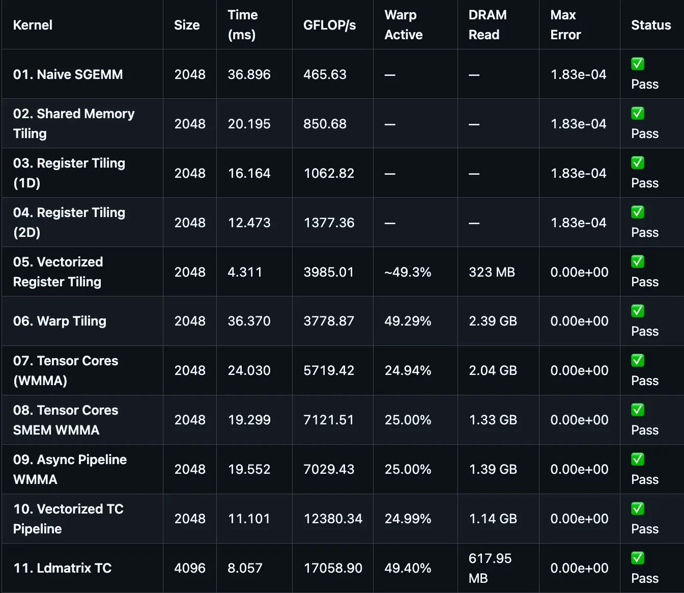
6. Benchmark Results
Benchmark: matrix dimensions M = N = K vary by kernel size indicated below. ncu metrics collected with --launch-skip 1 --launch-count 1 on a single steady-state invocation.
7. Conclusion
High-performance GEMM is not the result of one algorithmic trick. It emerges from a sequence of hardware-aligned structural changes, each one removing the constraint that was limiting the previous version.
What the data shows
The progression from v01 to v11 is not monotonically smooth. Three results stand out:
-
v06 (Warp Tiling) is slower than v05 (Vectorized Register Tiling) despite introducing warp-level output ownership — a concept that becomes essential for Tensor Cores. The ncu data explains why:
BK = 8forces 256 shared memory reload iterations per kernel call, generating 543 MB of DRAM traffic versus 276 MB for cuBLAS. Warp alignment reduces instruction-level conflicts but cannot compensate for a tile configuration that doubles memory traffic. The lesson: structural correctness and performance are independent — a kernel can have the right abstraction at the wrong scale. -
v10 (Vectorized TC Pipeline) is slower than v09 despite issuing 8× fewer memory instructions. The ncu explanation:
BLOCK_TILE_M = 32, BLOCK_TILE_N = 64produces only 64int4loads for the A tile across 256 threads — 75% of threads sit idle during every load phase. Vectorization and tile size are not separable optimizations. Reducing instruction count while simultaneously reducing in-flight memory requests makes the memory wall worse, not better. -
v11 (Ldmatrix TC) breaks the memory wall by combining the two missing pieces simultaneously: a
128×128×32tile that fully occupies all threads during vectorizedint4global loads, and PTXldmatrixthat loads shared-memory fragments into Tensor Core registers with a single warp-collective instruction. The result is17.06 TFLOP/s— a 5.7× jump over the previous peak (v10 at 3 TFLOP/s) and 26.2% of the65 TFLOP/sFP16 Tensor Core peak on the T4.
The pattern across all versions
Each optimization removes one bottleneck and exposes the next:
v01 → v02: repeated global memory reads        → replaced by shared memory tiling
v02 → v04: low arithmetic intensity             → replaced by register tiling
v04 → v05: high load instruction pressure       → replaced by float4 vectorization
v05 → v07: FP32 CUDA cores near peak            → replaced by FP16 Tensor Cores
v07 → v09: memory latency serialized with MMA   → replaced by double-buffer pipeline
v09 → v10: tile too small for vectorized loads  → MLP drops, throughput regresses
v10 → v11: wider tile + ldmatrix               → 17.06 TFLOP/s, memory wall breached
v11 → v12: synchronous Global→Shared stalls    → target: cp.async hardware pipeline
The journey from 465 GFLOP/s (v01) to 17.06 TFLOP/s (v11) demonstrates that no single technique delivers peak performance — each layer of the memory hierarchy and the instruction pipeline must be addressed in concert. The remaining ~74% gap from FP16 peak is the subject of v12 (Ampere cp.async) and v13 (Hopper TMA + WGMMA).
By tracing this full path from naive global-memory access to asynchronous Tensor Core pipelines — and verifying each claim with hardware counter data — this repository makes the trade-offs of modern GPU programming concrete, measurable, and reproducible.
If you prefer to read more detail in medium, you can access the link:
All rights reserved